Pdc Lab Manual 5g538
This document was ed by and they confirmed that they have the permission to share it. If you are author or own the copyright of this book, please report to us by using this report form. Report 3i3n4
Overview 26281t
& View Pdc Lab Manual as PDF for free.
More details 6y5l6z
- Words: 4,642
- Pages: 33
Pulse Circuits Lab
PART - II
PULSE CIRUITS LAB MANUAL
ATRI
Page 1
Pulse Circuits Lab
List of Experiments Part-II : PULSE CIRCUITS
1.
Linear Wave shaping Circuits
2.
Non Linear Wave shaping Circuits
3.
Comparison Operation of Comaparator
4.
Switching Characteristics of a Transistor
5.
Design a Bistable Multivibrator and draw its Waveforms
6.
Design a Astable Multivibrator and draw its Waveforms
7.
Design a Monostable Multivibrator and draw its Waveforms
8.
Response of Schmitt Trigger Circuit for a loop gain Less than and greater than one
9.
UJT relaxation Oscillator
10.
The output Voltage Waveform Of Boot strap Sweep Circuit
11.
The output Voltage Waveform Of Miller Sweep Circuit
ATRI
Page 2
Pulse Circuits Lab Expt.No:01
LINEAR WAVE SHAPING AIM: To observe the effect of time constant on the output wave form of an RC low & high filter.
APPARATUS: S.NO
NAME OF THE EQUIPMENT
QUANTITY
1
Decade resistance box
1
2
capacitor (0.1uf)
1
3
Function generator
1
4
C.R.O
1
5
Bread Board
1
CIRUIT DIAGRAM:
A. Low RC Circuit
ATRI
Page 3
Pulse Circuits Lab B. High RC Circuit
THEORY:
LOW RC CIRCUIT: When a square is applied to a low filter RC circuit t=0 output voltage at that instant is 0 as output is taken across capacitor, and a capacitor can’t change its voltage instantaneously. Now capacitor starts raising its voltage exponentially with time constant RC and hence the output voltage reaches the maximum value. There is a fall in the input voltage by an amount of “V” abruptly. Again capacitor can’t change. Its voltage instantaneously. Therefore the output voltage Vo starts falling exponentially with time constant RC and continues. So on as long as square wave applied at the input.
HIGH CIRCUIT: When a square wave is applied for a high RC circuit at t = 0, since voltage across the capacitor can’t change instantaneously the out put voltage across the resistor raises to input voltage ‘V’. As capacitor voltage increases exponentially out put voltage starts falling exponentially. When the output voltage reaches the maximum value, there is an abrupt fall in input voltage by an amount ‘V’. This cause a fall in output voltage by ‘V’ from previous level. Thus the response curve comes to a negative voltage again the output voltage starts falling exponentially. When it reaches to a maximum level, then raise in input causes raise in output and same thing repeats again.
PROCEDURE 1. Connections are made as per circuit diagram
ATRI
Page 4
Pulse Circuits Lab 2. Square wave input signal is applied to the integrator circuit and wave forms are noted with peak-peak amplitude and frequency is measured in each case RC<
>t. 3. Respective graphs are drawn for RC>>t, RC=t, RC<
For RC<
Vo =
c=0.1 u f R=1KΩ
T=
For RC=t t=1 m sec
Vo =
c=0.1 u f R=10kΩ
T=
For RC>>t T=1 m sec
Vo =
C=0.1 u f R=100Kω
T=
PRECAUTIONS:
1. Connections should be firm. 2. Readings are noted without parallax error. 3. Before switch on the power supply all the knobs of power supply set at zero position.
RESULT:
The effect of time constant on the output wave form of Rc circuits is observed in all cases i.e., RC<
>t.
ATRI
Page 5
Pulse Circuits Lab Expt.No:02
NON LINEAR WAVE SHAPING CLIPPERS AIM: To the response of different clipper circuits and draw the transmission characteristics of each clipping circuit.
APPARATUS:
S.NO.
EQUIPMENT
QUANTITY
1.
Diodes IN4007
2
2.
Resistors 1KΩ
1
3.
Function generator
1
4.
RPS
1
5.
CRO
1
SHUNT DIODE POSITIVE CLIPPER: In put R1 1.0k
V1
D1
t
1N4007GP 4V 1kHz 0Deg
Out put V2 1V
VR+Vr t
SHUNT DIODE NEGITIVE CLIPPER:
R2 output 1.0k
V3 4V 1kHz 0Deg
D2 1N4007GP
Out put VR-Vr V4 1V
ATRI
t
Page 6
Pulse Circuits Lab SERIES DIODE POSITIVE CLIPPER:
In put
D3 1N4007GP
t
R3 1.0k
V5
Out put
4V 1kHz 0Deg
V6
VR-Vr
1V
t
SERIES DIODE NEGATIVE CLIPPER:
D1 output V1
1N4007GP
R1 1.0k
4V 1kHz 0Deg
Out put V2
VR+Vr
1.5 V
t
CLIPPING AT TWO INDIPENDENT LEVELS:
output R2 1.0k
D2
D3
1N4007GP
1N4007GP
VR+Vr
V5 4V 1kHz 0Deg
ATRI
Out put V3
V4
1.5 V
1V
-(VR+Vr)
t
Page 7
Pulse Circuits Lab
THEORY: Clipping circuit basically limit the amplitude of the input signal applied to the either bellow or above a percent voltage level. They may also restrict the output wave forms to lie with in certain set voltage limits. Hence they are also called limiters or slicers. Their chief applications are to transmit that part of an arbitrary wave form, which lie above or below reference level.
PROCEDURE: 1. Make the connections as per the circuit diagram. 2. Observe the amplitude of the output wave for series and shunt diode clipping circuits using C.R.O and note down the wave forms. 3. Draw the corresponding output waveform graph.
For two level diode clipper: 1. VR1 and VR2 are selected such that VR2 ≠ VR1. 2. It is observed that the given sine wave is converted into an approximated rectangular waveform. 3. Corresponding graphs are drawn for the output waveform of two independent level clippers. RESULT:
The response of different clipping circuits is observed.
ATRI
Page 8
Pulse Circuits Lab
CLAMPERS AIM: To the response of different clamping circuits.
APPARATUS: S.NO
NAME OF THE EQUIPMENT
QUANTITY
1.
Diodes (IN4007)
1
2.
Capacitor (0.01) µf
1
3.
Regulated power supply
1
4.
C.R.O
1
5.
Function Generator
1
6.
Bread Board
1
In put CIRCUIT DIAGRAM: Positive Clamper C1 V1
0.1uF
4V 1kHz 0Deg
D1
1N4007GP Out put
Negative Clamper C2 0.1uF
V2 4V 1kHz 0Deg
ATRI
D2 1N4007GP
Out put
Page 9
Pulse Circuits Lab THEORY: Clamping circuit add a d c level to an a c signal, Basically they pull up the maximum level of the input signal to a present reference level Vr and then allow the output to follow the input. Thus the output is always maintained below reference voltage level V r. The basic principle of the circuit is illustrated in above figure. In the first quarter of the input cycle the capacitor charges up to the maximum amplitude Vm and the diode is forward bias. Assuming that its forward resistance Rf is zero. The output remains zero voltage during this first quarter and the capacitor quickly charges to Vm. In the second quarter the input signal voltage falls from Vm. The diode is now reverse biased. Its reverse resistance Rr can be assumed infinite. The capacitor having no discharge path remains charged at Vm. The plate of the capacitor connected to the output terminals is negative. Also if the source has a resistance as zero ohms. It suffers no voltage drop. Hence the output Vo Vm –Vm. The entire swing if the output is form 0V to -2Vm corresponding to Vin = +Vm to Vin = -Vm respectively. The clamping level goes down to – Vr i.e. the + Ve peaks of the input signal get clamping at –Vr volts.
PROCEDURE: 1. Connections are made as per the circuit diagram. 2. For observing clamping waveform the AC/DC push button switch was to be kept in D.C. mode. 3. Note the values of the amplitude for each circuit from the C.R.O. 4. The output waveform was to be drawn on the graph for each circuit.
PRECAUTIONS: 1. Connections should be firm. 2. Readings are noted without parallax error. 3. Before switch on the power supply all the knobs of power supply are to be set at zero position.
RESULT: The response of different clamping circuits is observed. ATRI
Page 10
Pulse Circuits Lab Expt.No:03
COMPARISON OPERATION OF COMAPARATOR
AIM: To study the operation Comparison Operation of Comaparator.
APPARATUS:
SNO
1. 2.
NAME OF THE EQUIPMENT
Bread board trainer C.R.O
QUANTITY
1 1
3.
Function Generator
1
6.
Resistors
1
7.
RPS
1
CIRCUIT DIAGRAM:
ATRI
Page 11
Pulse Circuits Lab PROCEDURE: 1. Connections are made as per the circuit diagram. 2. For observing clamping waveform the AC/DC push button switch was to be kept in D.C. mode. 3. Note the values of the amplitude for each circuit from the C.R.O. The output waveform was to be drawn on the graph for each circuit PRECAUTIONS: 1. Connections should be firm. 2. Readings are noted without parallax error. 3. Before switch on the power supply all the knobs of power supply are to be set at zero position.
RESULT: The response of different Comparison Operation of Comaparator is observed.
ATRI
Page 12
Pulse Circuits Lab Expt.No:04
TRANSISTOR AS A SWITCH AIM: To study the operation of transistor as a switch.
APPARATUS:
SNO
1. 2. 3. 4.
NAME OF THE EQUIPMENT
Bread board trainer
QUANTITY
1
C.R.O
1
Transistor (SL 100)
1
LED
1
5.
Function Generator
1
6.
Resistors 4.7k
1
7.
100k
1
CIRCUIT DIAGRAM:
V in VCC 9V
R2 4.7k
t Q1 R1 100k
V1
BC107BP
Output
V Out 100% 90%
2V 1kHz 0Deg
10%
tr td
ATRI
ts
t
tf td
Page 13
Pulse Circuits Lab THEORY: When transistor makes a transition from its cut off state, to the saturation state or ON state it takes a finite time to do so. It takes the finite time for the reserve transition from the ON to OFF state.
DELAY TIME:
This time is taken during turn ON. It is the time duration form the point when the input pulse at base of the transistor reaches 10 % of its maximum amplitude, to the point when the collector current charges from 0 to 10% of its maximum amplitude.
RISE TIME:
This time is also taken during turn ON; it is the time interval in which the collector current pulse changes from 10% to 90% of its maximum valve.
STORAGE TIME:
The time interval during turn off transition of the transistor is between the points when the input pulse at the base changes to 10%of its maximum amplitude, to the point when the collector current changes from 100% to 90% of collector current.
FALL TIME: The time interval at turn off during which the collector current decreases from 90% to 10% of its maximum amplitude is the fall time.
PROCEDURE:
1. All the connections are made as per circuit diagram. 2. Observe the out put wave form that appears on C.R.O. with peak-to-peak amplitude and frequency and note these values.
ATRI
Page 14
Pulse Circuits Lab 3. The delay time, rise time, storage time, fall time are calculated from their used definitions using the output waveform on C.R.O. 4. Switching action of transistor was observed by putting a led at output by reducing the frequency of input waveform. 5. The graph is plotted for the output waveform and the ON times OFF time are indicated. OBSERVATIONS:
td =
tr =
ts =
tf =
td =
PRECAUTIONS:
1. Connections should be firm. 2. Readings are noted without parallax error. 3. Before switch on the power supply all the knobs of power supply set at zero position. RESULT: 1. The switching action of transistor is observed efficiency. 2. Rise time, fall time, storage time, delay time are calculated. 3. The ON time and OFF time are noted.
ATRI
Page 15
Pulse Circuits Lab Expt.No:05
BISTABLE MULTIVIBRATOR AIM: To study and the output wave form of a Bistable Multivibrator.
APPARATUS:
S.NO
NAME
OF
THE
QUANTITY
EQUIPMENT 1
Transistor ( SL 100 / BC107)
2
2
Resistors
2
2.2KΩ 15 KΩ
2
100 KΩ
2
3
Capacitors 0.047µ F
2
4
CRO
1
5
Bread board
1
CIRCUIT DIAGRAM: Vb1 Vbe set
VCC 12V
R5
C2
C1
2.2k
t
R1 2.2k
0.047uF
0.047uF
R2
R4
15k
15k
Q2
Vb2 Vbe set t
Q1
BC107BP
R6 100k
BC107BP
Vc1
R3 100k
Vbb -1.5v
Vce set Vc2
t
Vce set t
ATRI
Page 16
Pulse Circuits Lab THEORY: The circuit has two stable states, and switches or vibrates between these two states on the application of external trigger, Hence it is turned as Bistable Multivibrator. These are two biasing voltages One for the collector circuit and another for the base circuit. The fixed bias to the collector is provided by VCC and RC. The fixed bias to base is provided by VBB and R1 and R2. OPERATION: Consider that the transistor Q1 is OFF and the transistor is ON, the collector voltage of the OFF transistor is given by VCC – VCE (Sat). In the OFF mode only a small amount of leakage current flow through the transistor. For ON transistor we have VCC = 0. With the application of appropriate triggering pulse the stable state of binary can be changed. PROCEDURE: 1. Take a bread board and connect the components as per circuit diagram. 2. Apply the supply voltage VCC = + 12 V and connect CRO at the base of Q1. 3. Note down the wave forms time period and amplitude of wave form at the base of Q1. 4. Repeat the same procedure to note down the wave forms at base of Q2. 5. Similarly note down the wave forms at VC1 & VC2 of Q1 & Q2 respectively. 6. Note down the VBE (Sat) and (VCE (Sat) voltages. 7. Draw the wave forms on a graph. PRACAUTIONS: 1. Connections should be firm. 2. Readings are noted without parallax error. 3. Before switch on the power supply all the knobs of power supply set at zero position. 4. Increase the power supply slowly. 5. After note down the readings switch off the power supply.
RESULT: Responses at the base and collector points of the Bistable Multivibrator are observed. ATRI
Page 17
Pulse Circuits Lab Expt.No:06
ASTABLE MULTIVIBRATOR AIM: To understand the response at base and collector points of the Astable Multivibrator
APPRATUS: S.NO
NAME OF THE EQUIPMENT
1
Transistor (BC 107)
2
Resistors
QUANTITY
2
2.2kΩ
2
15kΩ
2
3
Capacitor 0.04 µf
2
4
Regulated power supply
1
5
CRO
1
6
1
Bread board
CIRCUIT DIAGRAM: VC1 Vcc
VCC 12V
R4 2.2k
C1
R2
R3
15k
15k
R1 2.2k
C2
Vce sat VC2
0.047uF
t
0.047uF
Q2
Q1
BC107BP
BC107BP
Vce sat t VB2 Vbe sat t
VB1 Vbe sat
t
ATRI
Page 18
Pulse Circuits Lab THEORY: An Astable Multivibrator has no stable states. The two transistors switch alternately between two quasi stable states. No external trigger is required to effect this change and hence is called as free running Multivibrator. RC1& RC2 are the collector resistors for transistors Q1&Q2 respectively. C1&C2 are coupling capacitors. Resistor R1&R2 provide ON state base current to the transistor T1&T2 during saturation region.
OPERATION: At time t=0, when the power supply voltage gets applied, due to slight mismatch Ic1 flowing through Q1 is little more then the collector Ic2 of Q2. Thus rate of fall of Vc1 is more then that of Vc2. so Vc1< Vcc will make the base of Q2 negative. This make the collector voltage Vc2 increase towards Vcc. This increase in Vc2 will be transferred through capacitor C2 to the base of Q1 and increasing the condition in Q1. Thus when Astable Multivibrator is switched we have the following conditions.
Q1 is in saturation
Q2 is in off region
PROCEDURE:
1. Take a bread board and connect the components as per circuit diagram. 2. Apply the supply voltage vcc =+12v and connect the C.R.O at desired points to observe the wave forms. 3. Note down the wave forms time period, amplitude from C.R.O by connecting it at vc1, vc2, & vb2 respectively. 4. Calculate the frequency of wave forms. 5. Check whether theoretical and practical values are correct or not.
THEORETICAL VALUES:
R1 =15K=R2 C1=C2=0.047uf ATRI
Page 19
Pulse Circuits Lab TI=0.69 R1C1 T2=0.69R2C2 TOTAL TIME PERIOD =T=1.38 RC 0.97ms=1ms Frequency =1/T=1/1ms=1kHz PRACTICAL VALUES :
1. Time period at Q1=T1= 2. Time period at Q2=T2= 3. Total Time period T=T1+T2= 4. Frequency=1/T
RESULT:
The response at base and collector point of Astable Multivibrator is observed.
ATRI
Page 20
Pulse Circuits Lab Expt.No: 07
MONOSTABLE MULTIVIBRATOR AIM: To construct the transistor monostable Multivibrator and observe the response at base and collector points.
APPARATUS: S.NO
NAME OF TE EQUIPMENT
QUANTITY
1
Transistor (SL 100 or BC 107)
2
2
Resistors 1KΏ
2
10KΏ
2
100KΏ
1
3
Capacitors 0.047μF
2
4
Regulated power supply
1
5
CRO
1
6
Bread board
1
CIRCUIT DIAGRAM VCC 12V
R1
R5
1.0k
10k
Vc2
R4 C2
1.0k
0.047uF
C1
R3
Vceset
10k
0.047uF
t
Q1
Q2
BC107BP
BC107BP
Vb1 Vbe sat
R2
Vr t
100k
Vbb(-1.5v) t
ATRI
Page 21
Pulse Circuits Lab THEORY: The basic collector coupled monostable circuit is shown in figure. STABLE STATE: Normally Q2 is in the ON state. Because it gets a sufficient base current through R3.This causes Q1 to be in the OFF state as Q2 collector which fed to the base of Q1 is at its low Vcc saturation value. This is fact that a negative bias applied at the base of Q1 turns it OFF. This is to the stable state.
ENTRY TO QUASI STABLE STATE: Now if Q2 is forced to become off due to large external trigger applied at its base, its collector voltage rises sharply. This gives a positive voltage through the voltage divider network of R1 and R2 at the base of Q1. This is sufficient to over come. The effect of its negative bias and exceed the cut in voltage of it’s BE terminal it turn ON. The circuit has now extended a quasi stable state.
RETURN TO STABLE STATE: When Q1 turns ON, the capacitors find a convenient path to change up to VCC through R3 and Q1. If the capacitor is charging till the voltage at the base of Q2 exceeds its cut in voltage at this point Q2 turn ON again and Q2 turn OFF. The circuit returns to its stable state. During the quasi stable state the voltage at the collector of Q2 has a high VCC level. Thus a pulse is obtained. The width of the pulse is given by T = 0.69 R3 C.
PROCEDURE: 8. Take a bread board and connect the components as per circuit diagram. 9. Apply the supply voltage VCC = + 12 V and connect CRO at the base of Q1. 10. Note down the wave forms time period and amplitude of wave form at the base of Q1. 11. Repeat the same procedure to note down the wave forms at base of Q2. 12. Similarly note down the wave forms at VC1 & VC2 of Q1 & Q2 respectively. 13. Calculate the Quasi stable time period. ATRI
Page 22
Pulse Circuits Lab 14. Draw the wave forms on a graph RECORD OF OBSERVATION: THEORITICAL VALUES: R2 = 10 KΩ C2 = 0.047µ F tp = 0.69 R2 C2 PRACTICAL VALUES: δ= VBE (sat) =
Vγ = tp=
PRECAUTIONS: 1. Connections should be firm. 2. Readings are noted without parallax error. 3. Before switch on the power supply all the knobs of power supply set at zero position. 4. Increase the power supply slowly. 5. After note down the readings switch off the power supply RESULT: The responses at base and collector point of monostable Multivibrator are observed.
ATRI
Page 23
Pulse Circuits Lab Expt.No:08
SCHMITT TRIGGER AIM: To generate a square wave form by using Schmitt trigger circuit.
APPARATUS:
S.NO
NAME OF THE EQUIPMENT
1
QUANTITY
transistor (SL100)
2
2
820Ω
resistors
1
1.2k Ω
1
1k Ω
1
10k
2
150 Ω 3
1
capacitors 0.047µf
4
1
function generator
5
1
C.R.O
1
6
regulated power supply
1
7
bread board
1
CIRCUIT DIAGRAM VCC 4.5V
R1 C1
1.0k
Vin R6 1.0k
UTP LTP
0.047uF
R2 1.2k
Q1
t
Q2
R5 820 BC107BP
R3 10k
V out BC107BP
Vcc
V1 4V 1kHz 0Deg
R4 150
IeRe t
ATRI
Page 24
Pulse Circuits Lab THEORY: Schmitt trigger is a special type of Bistable Multivibrator. It differs from the basic binary circuit. In the basic circuit there won’t be any resistive coupling between the output of Q2 and the input of Q1. Although the collector of Q1and the base of Q2 are coupled in usual manner. The emitter of Q1 and Q2 are ed, and they are grounded through a common resistor Rc. The base of Q1is connected to a voltage source Vi. It should be noted that the output of a Schmitt trigger is a square wave what ever the wave form of the input signal.
PROCEDURE 1. Connections are made as for the circuit diagram. 2. Apply the supply voltage VCC = 4.5 V & connect the C.R.O at output terminals. 3. Apply the input square wave frequency 1KHZ and amplitude of 4V(P-P). 4. Observe the output wave form on C.R.O & note down the amplitude & time period
of
square wave form. 5. Sketch the waveform on graph sheet.
RECORD OF OBSERVATIONS: 1. The time period of square waveform 2. The amplitude of square waveform
PRECAUTIONS: 1. Connections should be tight. 2. Before switch on the power supply set the all knobs at zero positions. 3. Increase the power supply slowly and smoothly.
RESULT: Square wave is generated by using Schmitt trigger circuit.
ATRI
Page 25
Pulse Circuits Lab Expt.No:09
UJT RELAXATION OSCILLATOR AIM: To construct and study the operation of Uni junction transistor as a relaxation oscillator.
APPARTUS:
S.NO
NAME OF THE EQUIPMENT
QUANTITY
1.
Bread board trainer
1
2.
UJT 2N2646
1
3.
Resistors 330Ω
1
47Ω
1
4.
Decade resistance box
1
5.
Capacitor 0.1µf
1
CIRCUIT DIAGRAM:
10K _LIN Key = A
R3
Vb1
R2 330
Vb2
50%
t output Vp
2N2646
V out C1 0.1uF
ATRI
Vv
R1 47
Vb1 t
Page 26
Pulse Circuits Lab THEORY: The injunction transistor has only the P-N junction. it has a P-type emitter alloyed to lightly doped N type material. There are two bases, B1 and B2. Base B1 being closer to the emitter that base B2. The P-N junction is formed between the P-type emitter and N-type silicon bar. RB1 is the resistance between base B1 and the emitter, and it is a basically a variable resistance its value being dependent upon the emitter Ie. RB2 is the resistance between B2 and the emitter and its value is fixed. Vp =Vr +Vγ Vp = Vr + VBB
Vγ = VBB
It is Obvious that if VE < VP that UJT is OFF, If VE > VP the UJT is ON
VV =Valley Voltage,
VP = peak voltage.
It is seen that when the capacitor voltage VS rises to the value VP the UJT readily conducts. When the UJT becomes ON the capacitor discharges and its voltage falls. When the voltage falls to the valley point Vv. The UJT becomes OFF and the capacitor charges again to Vp. This cycle of charging and discharging of the capacitor C repeats and as a result a saw tooth waveform of voltage across C is generated.
The output across C shows in figure.
Ts = Sweep time Tr = Return time Tv= Valley time
PROCEDURE:
(1) Take bread broad and connect the component as per circuit diagram. (2) Connect VBB=15 and connect C.R.O across capacitor “C”.
ATRI
Page 27
Pulse Circuits Lab (3) Note down the waveform and connect C R O across RB1and RB2 and note down the wave forms (4) Calculate the time period and check whether it is equal to the theoretical value or not. (5) Sketch the wave forms on graph
RECORD OF OBSERVATIONS:
THEORITICAL VALUE: T = RC (log 1/ 1- ŋ)
PRACTICAL VALUE: T=
PRECAUTIONS:
1. Connections should be tight. 2. Readings are noted without parallel error. 3. Before switch on the power supply all the knobs of power supply should set at zero position. RESULT:
Response of the UJT Relaxation Oscillator is observed.
ATRI
Page 28
Pulse Circuits Lab Expt.No:10
BOOTSTRAP SWEEP CIRCUIT AIM: To study the working of bootstrap sweep circuit.
APPRATUS:
S.NO
NAME OF THE EQUIPMENT
QUANTITY
1
Transistor (SL100)
1
2
Resisters 1kΩ
1
1MΩ
1
3
Capacitors 100µf
1
1µf
1
4
Function generator
1
5
CRO
1
6
Regulated power supply
1
7
Bread board
1
CIRCUIT DIAGRAM:
+ Vcc 12 v V input
R1 1.0k
t
Q1
C1 100uF
4 V (P-P) 1Khz
Vs
BC107BP
V out
R2
C2
1.0M
1uF
t
ATRI
Page 29
Pulse Circuits Lab THEORY: The circuit is transistor base sweep circuit. The output sweep circuit is ramp voltage generally the sweep circuits are employed to trigger the horizontal amplifier of C R T’s in C R O’s sweep circuit is used in television sweep voltage trigger the horizontal amplifier.
A ramp voltage is obtained by allowing a constant current to flow through it. This is achieved by using the transistor as switch. When a transistor is ON it makes to flow a constant current through the output capacitor.
A capacitor and resister at the base of the transistor forms a differentiator circuit that produces spikes at the base of the transistor. The negative spikes make the transistor is off. These results in charging the output capacitor to Vcc through Rc1. thus the output voltage taken across the capacitor raises exponentially. When the positive excursion occurs at the base, the transistor will be ON. Thus the capacitor discharging through the transistor. Thus this cycle continues hence giving up a sweep wave form.
The output waveform is 180 ° out off phase of the input excitation signal since the transistor is in CE mode
PROCEDURE: 1. Connect the components as per circuit diagram. 2. Connect the Vcc = +12 v, and apply square wave of frequency 1 kHz and 4v (p-p) amplitude at the input terminals. 3. Take the output in CRO across the 1µf capacitor. 4. Observe the waveform on CRO 5. Note down the p-p amplitude and time period of the output sweep wave form. 6. Draw the input and output wave forms in graph RECORD OF OBSERVATION: Amplitude of sweep waveform: Time period of sweep waveform:
RESULT: The working of Bootstrap sweep circuit is studied. ATRI
Page 30
Pulse Circuits Lab Expt.No:11
MILLER SWEEP CIRCUIT
AIM: To study the working of Miller sweep circuit.
APPRATUS:
S.NO
NAME OF THE EQUIPMENT
1
Transistor (BC107)
2
Resisters
3
Capacitors
4
Function generator
5
CRO
6
Regulated power supply
7
Bread board
CIRCUIT DIAGRAM:
ATRI
Page 31
Pulse Circuits Lab
THEORY: The circuit is transistor base sweep circuit. The output sweep circuit is ramp voltage generally the sweep circuits are employed to trigger the horizontal amplifier of C R T’s in C R O’s sweep circuit is used in television sweep voltage trigger the horizontal amplifier.
A ramp voltage is obtained by allowing a constant current to flow through it. This is achieved by using the transistor as switch. When a transistor is ON it makes to flow a constant current through the output capacitor.
A capacitor and resister at the base of the transistor forms a differentiator circuit that produces spikes at the base of the transistor. The negative spikes make the transistor is off. These results in charging the output capacitor to Vcc through Rc1. thus the output voltage taken across the capacitor raises exponentially. When the positive excursion occurs at the base, the transistor will be ON. Thus the capacitor discharging through the transistor. Thus this cycle continues hence giving up a sweep wave form.
PROCEDURE:
ATRI
Page 32
Pulse Circuits Lab
1. Test all the components and set up the circuit. 2. Switch ON the VCC supply. Q1 is in ON state and Q2 is in OFF state by measuring the collector voltages. RECORD OF OBSERVATION: Amplitude of sweep waveform: Time period of sweep waveform:
RESULT: The working of Miller sweep circuit is studied. ATRI
Page 33
PART - II
PULSE CIRUITS LAB MANUAL
ATRI
Page 1
Pulse Circuits Lab
List of Experiments Part-II : PULSE CIRCUITS
1.
Linear Wave shaping Circuits
2.
Non Linear Wave shaping Circuits
3.
Comparison Operation of Comaparator
4.
Switching Characteristics of a Transistor
5.
Design a Bistable Multivibrator and draw its Waveforms
6.
Design a Astable Multivibrator and draw its Waveforms
7.
Design a Monostable Multivibrator and draw its Waveforms
8.
Response of Schmitt Trigger Circuit for a loop gain Less than and greater than one
9.
UJT relaxation Oscillator
10.
The output Voltage Waveform Of Boot strap Sweep Circuit
11.
The output Voltage Waveform Of Miller Sweep Circuit
ATRI
Page 2
Pulse Circuits Lab Expt.No:01
LINEAR WAVE SHAPING AIM: To observe the effect of time constant on the output wave form of an RC low & high filter.
APPARATUS: S.NO
NAME OF THE EQUIPMENT
QUANTITY
1
Decade resistance box
1
2
capacitor (0.1uf)
1
3
Function generator
1
4
C.R.O
1
5
Bread Board
1
CIRUIT DIAGRAM:
A. Low RC Circuit
ATRI
Page 3
Pulse Circuits Lab B. High RC Circuit
THEORY:
LOW RC CIRCUIT: When a square is applied to a low filter RC circuit t=0 output voltage at that instant is 0 as output is taken across capacitor, and a capacitor can’t change its voltage instantaneously. Now capacitor starts raising its voltage exponentially with time constant RC and hence the output voltage reaches the maximum value. There is a fall in the input voltage by an amount of “V” abruptly. Again capacitor can’t change. Its voltage instantaneously. Therefore the output voltage Vo starts falling exponentially with time constant RC and continues. So on as long as square wave applied at the input.
HIGH CIRCUIT: When a square wave is applied for a high RC circuit at t = 0, since voltage across the capacitor can’t change instantaneously the out put voltage across the resistor raises to input voltage ‘V’. As capacitor voltage increases exponentially out put voltage starts falling exponentially. When the output voltage reaches the maximum value, there is an abrupt fall in input voltage by an amount ‘V’. This cause a fall in output voltage by ‘V’ from previous level. Thus the response curve comes to a negative voltage again the output voltage starts falling exponentially. When it reaches to a maximum level, then raise in input causes raise in output and same thing repeats again.
PROCEDURE 1. Connections are made as per circuit diagram
ATRI
Page 4
Pulse Circuits Lab 2. Square wave input signal is applied to the integrator circuit and wave forms are noted with peak-peak amplitude and frequency is measured in each case RC<
For RC<
Vo =
c=0.1 u f R=1KΩ
T=
For RC=t t=1 m sec
Vo =
c=0.1 u f R=10kΩ
T=
For RC>>t T=1 m sec
Vo =
C=0.1 u f R=100Kω
T=
PRECAUTIONS:
1. Connections should be firm. 2. Readings are noted without parallax error. 3. Before switch on the power supply all the knobs of power supply set at zero position.
RESULT:
The effect of time constant on the output wave form of Rc circuits is observed in all cases i.e., RC<
ATRI
Page 5
Pulse Circuits Lab Expt.No:02
NON LINEAR WAVE SHAPING CLIPPERS AIM: To the response of different clipper circuits and draw the transmission characteristics of each clipping circuit.
APPARATUS:
S.NO.
EQUIPMENT
QUANTITY
1.
Diodes IN4007
2
2.
Resistors 1KΩ
1
3.
Function generator
1
4.
RPS
1
5.
CRO
1
SHUNT DIODE POSITIVE CLIPPER: In put R1 1.0k
V1
D1
t
1N4007GP 4V 1kHz 0Deg
Out put V2 1V
VR+Vr t
SHUNT DIODE NEGITIVE CLIPPER:
R2 output 1.0k
V3 4V 1kHz 0Deg
D2 1N4007GP
Out put VR-Vr V4 1V
ATRI
t
Page 6
Pulse Circuits Lab SERIES DIODE POSITIVE CLIPPER:
In put
D3 1N4007GP
t
R3 1.0k
V5
Out put
4V 1kHz 0Deg
V6
VR-Vr
1V
t
SERIES DIODE NEGATIVE CLIPPER:
D1 output V1
1N4007GP
R1 1.0k
4V 1kHz 0Deg
Out put V2
VR+Vr
1.5 V
t
CLIPPING AT TWO INDIPENDENT LEVELS:
output R2 1.0k
D2
D3
1N4007GP
1N4007GP
VR+Vr
V5 4V 1kHz 0Deg
ATRI
Out put V3
V4
1.5 V
1V
-(VR+Vr)
t
Page 7
Pulse Circuits Lab
THEORY: Clipping circuit basically limit the amplitude of the input signal applied to the either bellow or above a percent voltage level. They may also restrict the output wave forms to lie with in certain set voltage limits. Hence they are also called limiters or slicers. Their chief applications are to transmit that part of an arbitrary wave form, which lie above or below reference level.
PROCEDURE: 1. Make the connections as per the circuit diagram. 2. Observe the amplitude of the output wave for series and shunt diode clipping circuits using C.R.O and note down the wave forms. 3. Draw the corresponding output waveform graph.
For two level diode clipper: 1. VR1 and VR2 are selected such that VR2 ≠ VR1. 2. It is observed that the given sine wave is converted into an approximated rectangular waveform. 3. Corresponding graphs are drawn for the output waveform of two independent level clippers. RESULT:
The response of different clipping circuits is observed.
ATRI
Page 8
Pulse Circuits Lab
CLAMPERS AIM: To the response of different clamping circuits.
APPARATUS: S.NO
NAME OF THE EQUIPMENT
QUANTITY
1.
Diodes (IN4007)
1
2.
Capacitor (0.01) µf
1
3.
Regulated power supply
1
4.
C.R.O
1
5.
Function Generator
1
6.
Bread Board
1
In put CIRCUIT DIAGRAM: Positive Clamper C1 V1
0.1uF
4V 1kHz 0Deg
D1
1N4007GP Out put
Negative Clamper C2 0.1uF
V2 4V 1kHz 0Deg
ATRI
D2 1N4007GP
Out put
Page 9
Pulse Circuits Lab THEORY: Clamping circuit add a d c level to an a c signal, Basically they pull up the maximum level of the input signal to a present reference level Vr and then allow the output to follow the input. Thus the output is always maintained below reference voltage level V r. The basic principle of the circuit is illustrated in above figure. In the first quarter of the input cycle the capacitor charges up to the maximum amplitude Vm and the diode is forward bias. Assuming that its forward resistance Rf is zero. The output remains zero voltage during this first quarter and the capacitor quickly charges to Vm. In the second quarter the input signal voltage falls from Vm. The diode is now reverse biased. Its reverse resistance Rr can be assumed infinite. The capacitor having no discharge path remains charged at Vm. The plate of the capacitor connected to the output terminals is negative. Also if the source has a resistance as zero ohms. It suffers no voltage drop. Hence the output Vo Vm –Vm. The entire swing if the output is form 0V to -2Vm corresponding to Vin = +Vm to Vin = -Vm respectively. The clamping level goes down to – Vr i.e. the + Ve peaks of the input signal get clamping at –Vr volts.
PROCEDURE: 1. Connections are made as per the circuit diagram. 2. For observing clamping waveform the AC/DC push button switch was to be kept in D.C. mode. 3. Note the values of the amplitude for each circuit from the C.R.O. 4. The output waveform was to be drawn on the graph for each circuit.
PRECAUTIONS: 1. Connections should be firm. 2. Readings are noted without parallax error. 3. Before switch on the power supply all the knobs of power supply are to be set at zero position.
RESULT: The response of different clamping circuits is observed. ATRI
Page 10
Pulse Circuits Lab Expt.No:03
COMPARISON OPERATION OF COMAPARATOR
AIM: To study the operation Comparison Operation of Comaparator.
APPARATUS:
SNO
1. 2.
NAME OF THE EQUIPMENT
Bread board trainer C.R.O
QUANTITY
1 1
3.
Function Generator
1
6.
Resistors
1
7.
RPS
1
CIRCUIT DIAGRAM:
ATRI
Page 11
Pulse Circuits Lab PROCEDURE: 1. Connections are made as per the circuit diagram. 2. For observing clamping waveform the AC/DC push button switch was to be kept in D.C. mode. 3. Note the values of the amplitude for each circuit from the C.R.O. The output waveform was to be drawn on the graph for each circuit PRECAUTIONS: 1. Connections should be firm. 2. Readings are noted without parallax error. 3. Before switch on the power supply all the knobs of power supply are to be set at zero position.
RESULT: The response of different Comparison Operation of Comaparator is observed.
ATRI
Page 12
Pulse Circuits Lab Expt.No:04
TRANSISTOR AS A SWITCH AIM: To study the operation of transistor as a switch.
APPARATUS:
SNO
1. 2. 3. 4.
NAME OF THE EQUIPMENT
Bread board trainer
QUANTITY
1
C.R.O
1
Transistor (SL 100)
1
LED
1
5.
Function Generator
1
6.
Resistors 4.7k
1
7.
100k
1
CIRCUIT DIAGRAM:
V in VCC 9V
R2 4.7k
t Q1 R1 100k
V1
BC107BP
Output
V Out 100% 90%
2V 1kHz 0Deg
10%
tr td
ATRI
ts
t
tf td
Page 13
Pulse Circuits Lab THEORY: When transistor makes a transition from its cut off state, to the saturation state or ON state it takes a finite time to do so. It takes the finite time for the reserve transition from the ON to OFF state.
DELAY TIME:
This time is taken during turn ON. It is the time duration form the point when the input pulse at base of the transistor reaches 10 % of its maximum amplitude, to the point when the collector current charges from 0 to 10% of its maximum amplitude.
RISE TIME:
This time is also taken during turn ON; it is the time interval in which the collector current pulse changes from 10% to 90% of its maximum valve.
STORAGE TIME:
The time interval during turn off transition of the transistor is between the points when the input pulse at the base changes to 10%of its maximum amplitude, to the point when the collector current changes from 100% to 90% of collector current.
FALL TIME: The time interval at turn off during which the collector current decreases from 90% to 10% of its maximum amplitude is the fall time.
PROCEDURE:
1. All the connections are made as per circuit diagram. 2. Observe the out put wave form that appears on C.R.O. with peak-to-peak amplitude and frequency and note these values.
ATRI
Page 14
Pulse Circuits Lab 3. The delay time, rise time, storage time, fall time are calculated from their used definitions using the output waveform on C.R.O. 4. Switching action of transistor was observed by putting a led at output by reducing the frequency of input waveform. 5. The graph is plotted for the output waveform and the ON times OFF time are indicated. OBSERVATIONS:
td =
tr =
ts =
tf =
td =
PRECAUTIONS:
1. Connections should be firm. 2. Readings are noted without parallax error. 3. Before switch on the power supply all the knobs of power supply set at zero position. RESULT: 1. The switching action of transistor is observed efficiency. 2. Rise time, fall time, storage time, delay time are calculated. 3. The ON time and OFF time are noted.
ATRI
Page 15
Pulse Circuits Lab Expt.No:05
BISTABLE MULTIVIBRATOR AIM: To study and the output wave form of a Bistable Multivibrator.
APPARATUS:
S.NO
NAME
OF
THE
QUANTITY
EQUIPMENT 1
Transistor ( SL 100 / BC107)
2
2
Resistors
2
2.2KΩ 15 KΩ
2
100 KΩ
2
3
Capacitors 0.047µ F
2
4
CRO
1
5
Bread board
1
CIRCUIT DIAGRAM: Vb1 Vbe set
VCC 12V
R5
C2
C1
2.2k
t
R1 2.2k
0.047uF
0.047uF
R2
R4
15k
15k
Q2
Vb2 Vbe set t
Q1
BC107BP
R6 100k
BC107BP
Vc1
R3 100k
Vbb -1.5v
Vce set Vc2
t
Vce set t
ATRI
Page 16
Pulse Circuits Lab THEORY: The circuit has two stable states, and switches or vibrates between these two states on the application of external trigger, Hence it is turned as Bistable Multivibrator. These are two biasing voltages One for the collector circuit and another for the base circuit. The fixed bias to the collector is provided by VCC and RC. The fixed bias to base is provided by VBB and R1 and R2. OPERATION: Consider that the transistor Q1 is OFF and the transistor is ON, the collector voltage of the OFF transistor is given by VCC – VCE (Sat). In the OFF mode only a small amount of leakage current flow through the transistor. For ON transistor we have VCC = 0. With the application of appropriate triggering pulse the stable state of binary can be changed. PROCEDURE: 1. Take a bread board and connect the components as per circuit diagram. 2. Apply the supply voltage VCC = + 12 V and connect CRO at the base of Q1. 3. Note down the wave forms time period and amplitude of wave form at the base of Q1. 4. Repeat the same procedure to note down the wave forms at base of Q2. 5. Similarly note down the wave forms at VC1 & VC2 of Q1 & Q2 respectively. 6. Note down the VBE (Sat) and (VCE (Sat) voltages. 7. Draw the wave forms on a graph. PRACAUTIONS: 1. Connections should be firm. 2. Readings are noted without parallax error. 3. Before switch on the power supply all the knobs of power supply set at zero position. 4. Increase the power supply slowly. 5. After note down the readings switch off the power supply.
RESULT: Responses at the base and collector points of the Bistable Multivibrator are observed. ATRI
Page 17
Pulse Circuits Lab Expt.No:06
ASTABLE MULTIVIBRATOR AIM: To understand the response at base and collector points of the Astable Multivibrator
APPRATUS: S.NO
NAME OF THE EQUIPMENT
1
Transistor (BC 107)
2
Resistors
QUANTITY
2
2.2kΩ
2
15kΩ
2
3
Capacitor 0.04 µf
2
4
Regulated power supply
1
5
CRO
1
6
1
Bread board
CIRCUIT DIAGRAM: VC1 Vcc
VCC 12V
R4 2.2k
C1
R2
R3
15k
15k
R1 2.2k
C2
Vce sat VC2
0.047uF
t
0.047uF
Q2
Q1
BC107BP
BC107BP
Vce sat t VB2 Vbe sat t
VB1 Vbe sat
t
ATRI
Page 18
Pulse Circuits Lab THEORY: An Astable Multivibrator has no stable states. The two transistors switch alternately between two quasi stable states. No external trigger is required to effect this change and hence is called as free running Multivibrator. RC1& RC2 are the collector resistors for transistors Q1&Q2 respectively. C1&C2 are coupling capacitors. Resistor R1&R2 provide ON state base current to the transistor T1&T2 during saturation region.
OPERATION: At time t=0, when the power supply voltage gets applied, due to slight mismatch Ic1 flowing through Q1 is little more then the collector Ic2 of Q2. Thus rate of fall of Vc1 is more then that of Vc2. so Vc1< Vcc will make the base of Q2 negative. This make the collector voltage Vc2 increase towards Vcc. This increase in Vc2 will be transferred through capacitor C2 to the base of Q1 and increasing the condition in Q1. Thus when Astable Multivibrator is switched we have the following conditions.
Q1 is in saturation
Q2 is in off region
PROCEDURE:
1. Take a bread board and connect the components as per circuit diagram. 2. Apply the supply voltage vcc =+12v and connect the C.R.O at desired points to observe the wave forms. 3. Note down the wave forms time period, amplitude from C.R.O by connecting it at vc1, vc2, & vb2 respectively. 4. Calculate the frequency of wave forms. 5. Check whether theoretical and practical values are correct or not.
THEORETICAL VALUES:
R1 =15K=R2 C1=C2=0.047uf ATRI
Page 19
Pulse Circuits Lab TI=0.69 R1C1 T2=0.69R2C2 TOTAL TIME PERIOD =T=1.38 RC 0.97ms=1ms Frequency =1/T=1/1ms=1kHz PRACTICAL VALUES :
1. Time period at Q1=T1= 2. Time period at Q2=T2= 3. Total Time period T=T1+T2= 4. Frequency=1/T
RESULT:
The response at base and collector point of Astable Multivibrator is observed.
ATRI
Page 20
Pulse Circuits Lab Expt.No: 07
MONOSTABLE MULTIVIBRATOR AIM: To construct the transistor monostable Multivibrator and observe the response at base and collector points.
APPARATUS: S.NO
NAME OF TE EQUIPMENT
QUANTITY
1
Transistor (SL 100 or BC 107)
2
2
Resistors 1KΏ
2
10KΏ
2
100KΏ
1
3
Capacitors 0.047μF
2
4
Regulated power supply
1
5
CRO
1
6
Bread board
1
CIRCUIT DIAGRAM VCC 12V
R1
R5
1.0k
10k
Vc2
R4 C2
1.0k
0.047uF
C1
R3
Vceset
10k
0.047uF
t
Q1
Q2
BC107BP
BC107BP
Vb1 Vbe sat
R2
Vr t
100k
Vbb(-1.5v) t
ATRI
Page 21
Pulse Circuits Lab THEORY: The basic collector coupled monostable circuit is shown in figure. STABLE STATE: Normally Q2 is in the ON state. Because it gets a sufficient base current through R3.This causes Q1 to be in the OFF state as Q2 collector which fed to the base of Q1 is at its low Vcc saturation value. This is fact that a negative bias applied at the base of Q1 turns it OFF. This is to the stable state.
ENTRY TO QUASI STABLE STATE: Now if Q2 is forced to become off due to large external trigger applied at its base, its collector voltage rises sharply. This gives a positive voltage through the voltage divider network of R1 and R2 at the base of Q1. This is sufficient to over come. The effect of its negative bias and exceed the cut in voltage of it’s BE terminal it turn ON. The circuit has now extended a quasi stable state.
RETURN TO STABLE STATE: When Q1 turns ON, the capacitors find a convenient path to change up to VCC through R3 and Q1. If the capacitor is charging till the voltage at the base of Q2 exceeds its cut in voltage at this point Q2 turn ON again and Q2 turn OFF. The circuit returns to its stable state. During the quasi stable state the voltage at the collector of Q2 has a high VCC level. Thus a pulse is obtained. The width of the pulse is given by T = 0.69 R3 C.
PROCEDURE: 8. Take a bread board and connect the components as per circuit diagram. 9. Apply the supply voltage VCC = + 12 V and connect CRO at the base of Q1. 10. Note down the wave forms time period and amplitude of wave form at the base of Q1. 11. Repeat the same procedure to note down the wave forms at base of Q2. 12. Similarly note down the wave forms at VC1 & VC2 of Q1 & Q2 respectively. 13. Calculate the Quasi stable time period. ATRI
Page 22
Pulse Circuits Lab 14. Draw the wave forms on a graph RECORD OF OBSERVATION: THEORITICAL VALUES: R2 = 10 KΩ C2 = 0.047µ F tp = 0.69 R2 C2 PRACTICAL VALUES: δ= VBE (sat) =
Vγ = tp=
PRECAUTIONS: 1. Connections should be firm. 2. Readings are noted without parallax error. 3. Before switch on the power supply all the knobs of power supply set at zero position. 4. Increase the power supply slowly. 5. After note down the readings switch off the power supply RESULT: The responses at base and collector point of monostable Multivibrator are observed.
ATRI
Page 23
Pulse Circuits Lab Expt.No:08
SCHMITT TRIGGER AIM: To generate a square wave form by using Schmitt trigger circuit.
APPARATUS:
S.NO
NAME OF THE EQUIPMENT
1
QUANTITY
transistor (SL100)
2
2
820Ω
resistors
1
1.2k Ω
1
1k Ω
1
10k
2
150 Ω 3
1
capacitors 0.047µf
4
1
function generator
5
1
C.R.O
1
6
regulated power supply
1
7
bread board
1
CIRCUIT DIAGRAM VCC 4.5V
R1 C1
1.0k
Vin R6 1.0k
UTP LTP
0.047uF
R2 1.2k
Q1
t
Q2
R5 820 BC107BP
R3 10k
V out BC107BP
Vcc
V1 4V 1kHz 0Deg
R4 150
IeRe t
ATRI
Page 24
Pulse Circuits Lab THEORY: Schmitt trigger is a special type of Bistable Multivibrator. It differs from the basic binary circuit. In the basic circuit there won’t be any resistive coupling between the output of Q2 and the input of Q1. Although the collector of Q1and the base of Q2 are coupled in usual manner. The emitter of Q1 and Q2 are ed, and they are grounded through a common resistor Rc. The base of Q1is connected to a voltage source Vi. It should be noted that the output of a Schmitt trigger is a square wave what ever the wave form of the input signal.
PROCEDURE 1. Connections are made as for the circuit diagram. 2. Apply the supply voltage VCC = 4.5 V & connect the C.R.O at output terminals. 3. Apply the input square wave frequency 1KHZ and amplitude of 4V(P-P). 4. Observe the output wave form on C.R.O & note down the amplitude & time period
of
square wave form. 5. Sketch the waveform on graph sheet.
RECORD OF OBSERVATIONS: 1. The time period of square waveform 2. The amplitude of square waveform
PRECAUTIONS: 1. Connections should be tight. 2. Before switch on the power supply set the all knobs at zero positions. 3. Increase the power supply slowly and smoothly.
RESULT: Square wave is generated by using Schmitt trigger circuit.
ATRI
Page 25
Pulse Circuits Lab Expt.No:09
UJT RELAXATION OSCILLATOR AIM: To construct and study the operation of Uni junction transistor as a relaxation oscillator.
APPARTUS:
S.NO
NAME OF THE EQUIPMENT
QUANTITY
1.
Bread board trainer
1
2.
UJT 2N2646
1
3.
Resistors 330Ω
1
47Ω
1
4.
Decade resistance box
1
5.
Capacitor 0.1µf
1
CIRCUIT DIAGRAM:
10K _LIN Key = A
R3
Vb1
R2 330
Vb2
50%
t output Vp
2N2646
V out C1 0.1uF
ATRI
Vv
R1 47
Vb1 t
Page 26
Pulse Circuits Lab THEORY: The injunction transistor has only the P-N junction. it has a P-type emitter alloyed to lightly doped N type material. There are two bases, B1 and B2. Base B1 being closer to the emitter that base B2. The P-N junction is formed between the P-type emitter and N-type silicon bar. RB1 is the resistance between base B1 and the emitter, and it is a basically a variable resistance its value being dependent upon the emitter Ie. RB2 is the resistance between B2 and the emitter and its value is fixed. Vp =Vr +Vγ Vp = Vr + VBB
Vγ = VBB
It is Obvious that if VE < VP that UJT is OFF, If VE > VP the UJT is ON
VV =Valley Voltage,
VP = peak voltage.
It is seen that when the capacitor voltage VS rises to the value VP the UJT readily conducts. When the UJT becomes ON the capacitor discharges and its voltage falls. When the voltage falls to the valley point Vv. The UJT becomes OFF and the capacitor charges again to Vp. This cycle of charging and discharging of the capacitor C repeats and as a result a saw tooth waveform of voltage across C is generated.
The output across C shows in figure.
Ts = Sweep time Tr = Return time Tv= Valley time
PROCEDURE:
(1) Take bread broad and connect the component as per circuit diagram. (2) Connect VBB=15 and connect C.R.O across capacitor “C”.
ATRI
Page 27
Pulse Circuits Lab (3) Note down the waveform and connect C R O across RB1and RB2 and note down the wave forms (4) Calculate the time period and check whether it is equal to the theoretical value or not. (5) Sketch the wave forms on graph
RECORD OF OBSERVATIONS:
THEORITICAL VALUE: T = RC (log 1/ 1- ŋ)
PRACTICAL VALUE: T=
PRECAUTIONS:
1. Connections should be tight. 2. Readings are noted without parallel error. 3. Before switch on the power supply all the knobs of power supply should set at zero position. RESULT:
Response of the UJT Relaxation Oscillator is observed.
ATRI
Page 28
Pulse Circuits Lab Expt.No:10
BOOTSTRAP SWEEP CIRCUIT AIM: To study the working of bootstrap sweep circuit.
APPRATUS:
S.NO
NAME OF THE EQUIPMENT
QUANTITY
1
Transistor (SL100)
1
2
Resisters 1kΩ
1
1MΩ
1
3
Capacitors 100µf
1
1µf
1
4
Function generator
1
5
CRO
1
6
Regulated power supply
1
7
Bread board
1
CIRCUIT DIAGRAM:
+ Vcc 12 v V input
R1 1.0k
t
Q1
C1 100uF
4 V (P-P) 1Khz
Vs
BC107BP
V out
R2
C2
1.0M
1uF
t
ATRI
Page 29
Pulse Circuits Lab THEORY: The circuit is transistor base sweep circuit. The output sweep circuit is ramp voltage generally the sweep circuits are employed to trigger the horizontal amplifier of C R T’s in C R O’s sweep circuit is used in television sweep voltage trigger the horizontal amplifier.
A ramp voltage is obtained by allowing a constant current to flow through it. This is achieved by using the transistor as switch. When a transistor is ON it makes to flow a constant current through the output capacitor.
A capacitor and resister at the base of the transistor forms a differentiator circuit that produces spikes at the base of the transistor. The negative spikes make the transistor is off. These results in charging the output capacitor to Vcc through Rc1. thus the output voltage taken across the capacitor raises exponentially. When the positive excursion occurs at the base, the transistor will be ON. Thus the capacitor discharging through the transistor. Thus this cycle continues hence giving up a sweep wave form.
The output waveform is 180 ° out off phase of the input excitation signal since the transistor is in CE mode
PROCEDURE: 1. Connect the components as per circuit diagram. 2. Connect the Vcc = +12 v, and apply square wave of frequency 1 kHz and 4v (p-p) amplitude at the input terminals. 3. Take the output in CRO across the 1µf capacitor. 4. Observe the waveform on CRO 5. Note down the p-p amplitude and time period of the output sweep wave form. 6. Draw the input and output wave forms in graph RECORD OF OBSERVATION: Amplitude of sweep waveform: Time period of sweep waveform:
RESULT: The working of Bootstrap sweep circuit is studied. ATRI
Page 30
Pulse Circuits Lab Expt.No:11
MILLER SWEEP CIRCUIT
AIM: To study the working of Miller sweep circuit.
APPRATUS:
S.NO
NAME OF THE EQUIPMENT
1
Transistor (BC107)
2
Resisters
3
Capacitors
4
Function generator
5
CRO
6
Regulated power supply
7
Bread board
CIRCUIT DIAGRAM:
ATRI
Page 31
Pulse Circuits Lab
THEORY: The circuit is transistor base sweep circuit. The output sweep circuit is ramp voltage generally the sweep circuits are employed to trigger the horizontal amplifier of C R T’s in C R O’s sweep circuit is used in television sweep voltage trigger the horizontal amplifier.
A ramp voltage is obtained by allowing a constant current to flow through it. This is achieved by using the transistor as switch. When a transistor is ON it makes to flow a constant current through the output capacitor.
A capacitor and resister at the base of the transistor forms a differentiator circuit that produces spikes at the base of the transistor. The negative spikes make the transistor is off. These results in charging the output capacitor to Vcc through Rc1. thus the output voltage taken across the capacitor raises exponentially. When the positive excursion occurs at the base, the transistor will be ON. Thus the capacitor discharging through the transistor. Thus this cycle continues hence giving up a sweep wave form.
PROCEDURE:
ATRI
Page 32
Pulse Circuits Lab
1. Test all the components and set up the circuit. 2. Switch ON the VCC supply. Q1 is in ON state and Q2 is in OFF state by measuring the collector voltages. RECORD OF OBSERVATION: Amplitude of sweep waveform: Time period of sweep waveform:
RESULT: The working of Miller sweep circuit is studied. ATRI
Page 33
Related Documents 3h463d

Pdc Lab Manual 5g538
January 2022 0
117766110-pdc-lab-manual 4 4evk
November 2019 25
Informe Lab. Pdc I 4v3644
September 2021 0
Pdc Chilca 231632
October 2020 0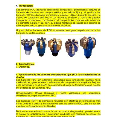
Trepanos Pdc 5v6q6w
April 2020 20
Pdc Huancan 5tz11
November 2020 0More Documents from "Bhanu Sri" 5p5de

Disha General Science Notes.pdf 621o61
April 2020 25
Pdc Lab Manual 5g538
January 2022 0
Guddalo Sulli d162l
December 2019 405
Otba Of Class 9 Of Maths 73285p
November 2019 62
G.o.ms.no.26 z5b2
December 2019 56